- 您现在的位置:买卖IC网 > Sheet目录325 > FAN3278TMX (Fairchild Semiconductor)IC BRIDGE DVR P-N 2A 30V 8-SOIC
�� �
�
�Applications� Information�
�Input� Thresholds�
�The� FAN3278� driver� has� TTL� input� thresholds� and�
�provides� buffer� and� level� translation� functions� from�
�logic� inputs.� The� input� thresholds� meet� industry-�
�standard� TTL-logic� thresholds,� independent� of� the� V� DD�
�voltage,� and� there� is� a� hysteresis� voltage� of�
�approximately� 0.4V.� These� levels� permit� the� inputs� to�
�be� driven� from� a� range� of� input� logic� signal� levels� for�
�which� a� voltage� over� 2V� is� considered� logic� HIGH.� The�
�driving� signal� for� the� TTL� inputs� should� have� fast� rising�
�and� falling� edges� with� a� slew� rate� of� 6V/μs� or� faster,� so�
�a� rise� time� from� 0� to� 3.3V� should� be� 550ns� or� less.�
�With� reduced� slew� rate,� circuit� noise� could� cause� the�
�driver� input� voltage� to� exceed� the� hysteresis� voltage�
�and� retrigger� the� driver� input� inadvertently.�
�Static� Supply� Current�
�In� the� I� DD� (static)� typical� performance� characteristics�
�(see� Figure� 7� and� Figure� 8)� ,� the� curve� is� produced� with�
�all� inputs� /� enables� floating� (OUTA� is� LOW,� OUTB� is�
�HIGH)� and� indicates� the� lowest� static� I� DD� current� for� the�
�tested� configuration.� For� other� states,� additional� current�
�flows� through� the� 100k� Ω� resistors� on� the� inputs� and�
�outputs,� shown� in� the� block� diagram� (see� Figure� 4)� .� In�
�these� cases,� the� static� I� DD� current� is� the� value� obtained�
�from� the� curves� plus� this� additional� current.�
�Gate� Drive� Regulator�
�FAN3278� incorporates� internal� regulators� to� regulate� the�
�gate� drive� voltage.� The� output� pin� slew� rate� is�
�determined� by� this� gate� drive� voltage� and� the� load� on�
�the� output.� It� is� not� user� adjustable,� but� a� series� resistor�
�can� be� added� if� a� slower� rise� or� fall� time� is� needed� at�
�the� MOSFET� gate.�
�Startup� Operation�
�The� FAN3278� startup� logic� is� optimized� to� drive� a� ground-�
�referenced� N-channel� MOSFET� with� channel� A� and� a�
�V� DD� -referenced� P-channel� MOSFET� with� channel� B.�
�The� optimum� operating� voltage� of� the� FAN3278� is� 8V� to�
�27V.� It� has� an� internal� “watchdog”� circuit� that� provides� a�
�loose� UVLO� turn-on� voltage� (V� ON� )� of� approximately� 3.8V�
�with� a� small� hysteresis� of� about� 10mV.� However,� it� is�
�recommended� that� V� DD� is� greater� than� 4.75V� in� all�
�application� circuits.�
�When� the� V� DD� supply� voltage� is� below� the� level� needed�
�to� operate� the� internal� circuitry,� the� outputs� are� biased�
�to� hold� the� external� MOSFETs� in� OFF� state.� Internal�
�100k� ?� resistors� bias� the� non-inverting� output� LOW� and�
�the� inverting� output� to� V� DD� to� keep� the� external�
�MOSFETs� off� during� startup� intervals� when� input� control�
�signals� may� not� be� present.�
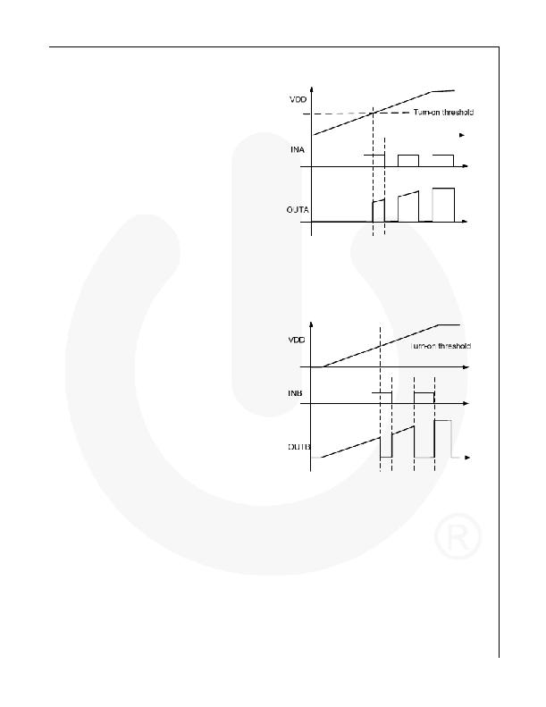
�Figure� 18� shows� startup� waveforms� for� non-inverting�
�channel� A.� At� power-up,� the� driver� output� for� channel� A�
�remains� LOW� until� V� DD� reaches� the� voltage� where� the�
�device� starts� operating,� then� OUTA� operates� in-phase�
�with� INA.�
�?� 2010� Fairchild� Semiconductor� Corporation�
�FAN3278� ?� Rev.� 1.0.1�
�10�
�Figure� 18.� Non-Inverting� Startup� Waveforms�
�Figure� 19� illustrates� startup� waveforms� for� inverting�
�channel� B.� At� power-up,� the� driver� output� for� channel� B�
�is� tied� to� V� DD� through� an� internal� 100k� ?� resistor� until�
�V� DD� reaches� the� voltage� where� the� device� starts�
�operating,� then� OUTB� operates� out� of� phase� with� INB.�
�Figure� 19.� Inverting� Startup� Waveforms�
�It� is� possible,� during� startup,� before� V� DD� has� reached�
�approximately� 4.5V,� that� the� output� pulse� width� may�
�take� a� few� switching� cycles� to� reach� the� full� duty-cycle�
�of� the� input� pulse.� This� is� due� to� internal� propagation�
�delays� affecting� the� operation� with� higher� switching�
�frequency� (e.g.� >100kHz)� and� slow� V� DD� ramp-up� (e.g.�
�<20V/ms).� For� this� reason,� it� is� recommended� that� V� DD�
�should� be� greater� than� 4.75V� before� any� INA� or� INB�
�signals� are� present.�
�For� high-frequency� applications� (several� hundred� kHz�
�up� to� 1MHz),� where� the� above� recommendation� of� V� DD�
�>4.75V� is� not� possible,� the� use� of� ENABLES� to� actively�
�hold� the� outputs� LOW� until� V� DD� >4.75V� assures� the�
�driver� output� pulse� width� follows� the� input� from� 4.75V�
�up� to� 28V.�
�www.fairchildsemi.com�
�发布紧急采购,3分钟左右您将得到回复。
相关PDF资料
FAN5331SX
IC LED DRVR WHITE BCKLGT SOT23-5
FAN5333ASX
IC LED DRVR WHITE BCKLGT SOT23-5
FAN5340MPX
IC LED DVR SYNC CC 8-MLP
FAN5341UMPX
IC LED DVR BOOST W/DIO 6-ULMP
FAN5343UMPX
IC LED DVR 6LED 500MW 6UMLP
FAN5345S30X
IC LED DVR ASYNC BOOST 30V 6SSOT
FAN5346S30X
IC LED DVR ASYNC SER BOOST 6SSOT
FAN53540UCX
IC REG SYNC BUCK 5A 20WLCSP
相关代理商/技术参数
FAN3506
功能描述:电流和电力监控器、调节器 Sec Side Control IC PC SMPS
RoHS:否 制造商:STMicroelectronics 产品:Current Regulators 电源电压-最大:48 V 电源电压-最小:5.5 V 工作温度范围:- 40 C to + 150 C 安装风格:SMD/SMT 封装 / 箱体:HPSO-8 封装:Reel
FAN3800
制造商:FAIRCHILD 制造商全称:Fairchild Semiconductor 功能描述:Mono / Stereo Audio Amplifier with Microphone Pre-Amplifier and EMU Interface
FAN3800_CAB3026B WAF
制造商:Fairchild Semiconductor Corporation 功能描述:
FAN3800_CAB3086B WAF
制造商:Fairchild Semiconductor Corporation 功能描述:
FAN3800MLP24
功能描述:音频放大器 DDR and ACPI Regulator RoHS:否 制造商:STMicroelectronics 产品:General Purpose Audio Amplifiers 输出类型:Digital 输出功率: THD + 噪声: 工作电源电压:3.3 V 电源电流: 最大功率耗散: 最大工作温度: 安装风格:SMD/SMT 封装 / 箱体:TQFP-64 封装:Reel
FAN3800MLP24X
功能描述:音频放大器 Mono & Stereo WITH MICROPHONE RoHS:否 制造商:STMicroelectronics 产品:General Purpose Audio Amplifiers 输出类型:Digital 输出功率: THD + 噪声: 工作电源电压:3.3 V 电源电流: 最大功率耗散: 最大工作温度: 安装风格:SMD/SMT 封装 / 箱体:TQFP-64 封装:Reel
FAN3850A
制造商:FAIRCHILD 制造商全称:Fairchild Semiconductor 功能描述:Microphone Pre-Amplifier with Digital Output
FAN3850AUC16X
功能描述:传声器前置放大器 Microphone Pre-Amp w/Digital Output
RoHS:否 制造商:Texas Instruments 可用增益调整:Digital control, 65 dB to 0 dB 共模抑制比(最小值): 输入补偿电压: 最大输入电阻:9200 Ohms 最大工作温度:+ 85 C 封装 / 箱体:SSOP-28 封装:Tube